


2020 kavli prize in Nanoscience
2020 Kavli
Prize in
Nanoscience
![Aberration-corrected transmission electron microscopy image of a thin film of the relaxor ferroelectric Ca0.28Ba0.72nb2O6on a srtiO3 substrate (in false colours). Both the amorphous area on the left (with predominant green colour), created by ion milling during processing, and the complex structure of the material viewed from the [001] crystallographic axis are clearly resolved. image courtesy of Chun-lin Jia.](https://cdn.sanity.io/images/qpjzy3y9/production/08a9dcaeba72281a084a63e3460ebeaf5fd8032f-2598x979.jpg?w=3840&q=75&fit=clip&auto=format)
The Norwegian Academy of Science and Letters has decided to award the 2020 Kavli Prize in Nanoscience to Harald Rose, Maximilian Haider, Knut Urban and Ondrej L. Krivanek.


For sub-ångström resolution imaging and chemical analysis using electron beams.
Committee Members
- Bodil Holst (Chair), University of Bergen, Norway
- Gabriel Aeppli, Paul Scherrer Institut, Switzerland
- Susan Coppersmith, University of New South Wales, Australia
- Shuit-Tong Lee, Soochow University, China
- Joachim Spatz, Max Planck Institute for Medical Research, Germany
Citation from the commitee
Seeing leads to scientific advancement, understanding and engineering. The 2020 Kavli Prize in Nanoscience honours four pioneers who enabled humanity to see the structure and chemical composition of materials in three dimensions on unprecedentedly short length scales.
A major goal of nanoscience is to create materials and devices assembled with atomic scale precision to obtain novel functionalities. The size of an atom is around one ångström (0.1 nanometer). Therefore, imaging and analysis of materials and devices at the sub-ångström scale is crucial. The resolution of a classical microscope is limited by the wavelength of the probe used for imaging. Because visible light has a wavelength around 5000 times larger than an atom, optical lenses cannot image atoms. In the early part of the 20th century beams of electrons with atomic scale wavelength became available, leading to the invention of the electron microscope in 1931. However, making ideal lenses for electrons turns out to be a big theoretical and experimental problem because lens aberrations limit the resolution. For more than 60 years people struggled! Through persistence, ingenuity and exploitation of the increase in computational power in the 1990s the Laureates constructed aberration corrected lenses and made sub-ångström imaging and chemical analysis in three dimensions a standard characterization method.
Three of the laureates co-founded two companies and commercialized their lenses contributing further to the major impact of their scientific work. Since then their microscopes have played an enormous role both in fundamental science and technology, where they are used, among others, by semiconductor, chemical and automotive industries.
The 2020 Kavli Prize Laureates in Nanoscience are
Harald Rose, for proposing a novel lens design, the Rose corrector, enabling aberration correction in transmission electron microscopy that can be applied to both conventional and scanning microscopes.
Maximilian Haider, for the realization of the first sextupole corrector, based on Rose’s design, and for his role in the implementation of the first aberration corrected conventional transmission electron microscope.
Knut Urban, for his role in the implementation of the first aberration corrected conventional transmission electron microscope.
Ondrej L. Krivanek, for the realization of the first aberration corrected scanning transmission electron microscope with sub-ångström resolution, well suited for spatially resolved chemical analysis. This was obtained using a quadrupole-octupole corrector.
Aberration-corrected transmission electron microscopy image of a thin film of the relaxor ferroelectric Ca0.28Ba0.72nb2O6on a srtiO3 substrate (in false colors). Both the amorphous area on the left (with predominant green color), created by ion milling during processing, and the complex structure of the material viewed from the [001] crystallographic axis are clearly resolved. Image courtesy of Chun-lin Jia.
Looking inside matter atom by atom
Manipulating matter at very small scales — even as precisely as moving single atoms — to create particles and devices with new functionalities is the ultimate ambition of nanoscience and nanotechnology. None of this could be achieved without an imaging technique that allows materials and devices to be studied with atomic resolution.
By Fabio Pulizzi
In making their award, the Kavli Prize in Nanoscience committee has selected four scientists who contributed to the development and use of two types of instrument, generally known collectively as aberration-corrected transmission electron microscopes, which can provide information about the structure and other properties of materials with sub-ångström resolution, hence allowing individual atoms to be distinguished.

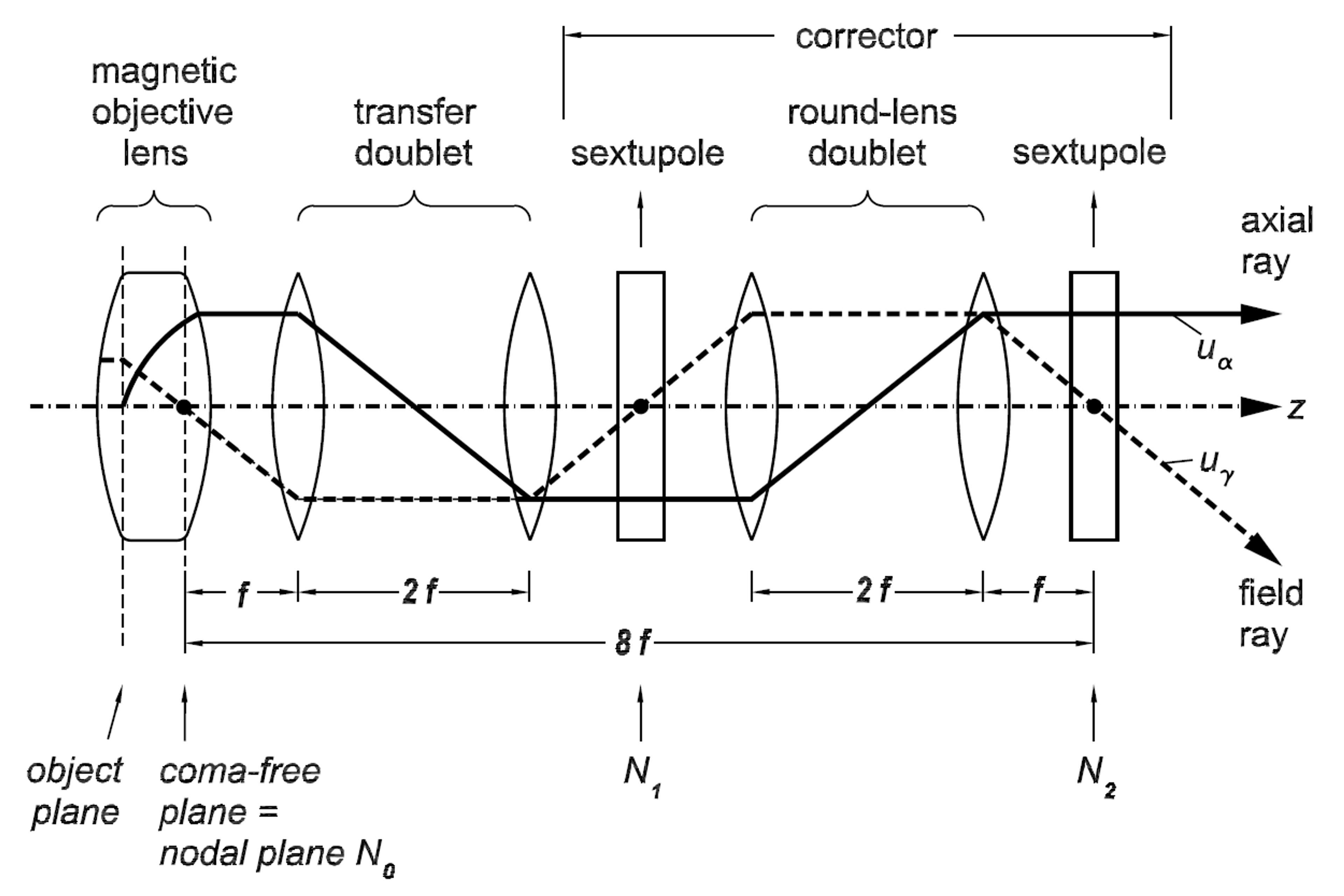
Figure 1. The schematic for an aberration corrector in the 1990 paper by Harald Rose. Optik 85, 19–24 (1990); © Elsevier GmbH
Optical microscopes can at best resolve features a few hundred nanometres across, so a different approach is necessary to distinguish single atoms. The scanning tunnelling microscope and the atomic force microscope, invented in the 1980s, achieved atomic resolution. However, they both work only on exposed surfaces, and for the majority of nanoscale structures it is essential to study the buried interfaces between different materials or different phases of the same material. The most promising route was to optimize the transmission electron microscope, invented in 1931 by Ernst Ruska. The instrument is based on the use of a beam of electrons directed at a thin sample of a given material. Interaction of the beam with the atoms in the material scatters the electrons. Using the scattered electrons the electromagnetic objective lens of the microscope and additional lenses form a magnified image which is recorded with a CCD or a CMOS camera. Ruska’s design is today called CTEM, for conventional transmission electron microscope. Conventional” means that, apart from employing electron radiation, CTEM follows the design of an optical microscope. In 1937 Manfred von Ardenne invented the scanning transmission electron microscope, the STEM. In this case, the specimen is scanned with a fine electron beam, collimated by the electromagnetic lenses, and the electrons that have passed through the specimen are collected behind it. The image is then created by displaying the intensity of these electrons on a video screen.
A unique advantage of the STEM is that for each spot of the material that the beam focuses on, it is also possible to analyse the energy lost by electrons when the beam scatters from atoms in the material. This technique, known as electron energy loss spectroscopy, or EELS, can provide information on the atomic composition and electronic states inside the material.
Although for both CTEM and STEM the resolution had reached a few ångströms by the late 1980s, it was impossible to resolve the detailed atomic arrangements in most materials. The problem was that the electromagnetic lenses being used suffered from aberrations much more than optical lenses do. So, for example, electrons passing through the lens far from the centre of it would be focused at a different distance from those traversing it close to the centre, thus blurring the images.
In 1990, Harald Rose, then at the University of Darmstadt, building on previous work on various ideas for aberration correction, designed a lens system based on electromagnetic hexapoles (Figure 1) that could be tuned to cancel the aberration of a standard electron lens, and that could work with both CTEM and STEM. In the following years, Rose teamed up with experimentalists Maximilian Haider, then based in Heidelberg, and Knut Urban in Jülich, to realize his proposal experimentally for a CTEM. In 1998, the collaboration resulted in the publication of the first images improved using an aberration-corrected CTEM. In 1996 Haider together with Joachim Zach had founded the company CEOS (Correlated Electron Optical Systems) to commercialize the ‘Rose corrector’, which is widely used today, in both CTEM and STEM.
Aberration-corrected CTEMs have developed substantially in the past 20 years, with the resolution now reaching 0.5 Å. Hence, in comparison with an uncorrected TEM the resolution with respect to the wavelength of electrons could be improved by a factor of 7. The ability to look at single atoms within a lattice has allowed the relationship between the local atomic structure and the properties of the material to be studied. A beautiful example is shown in Figure 2, in which an aberration-corrected TEM has been used to directly link the position of the atoms in a classic ferroelectric material to changes in electric polarization direction.

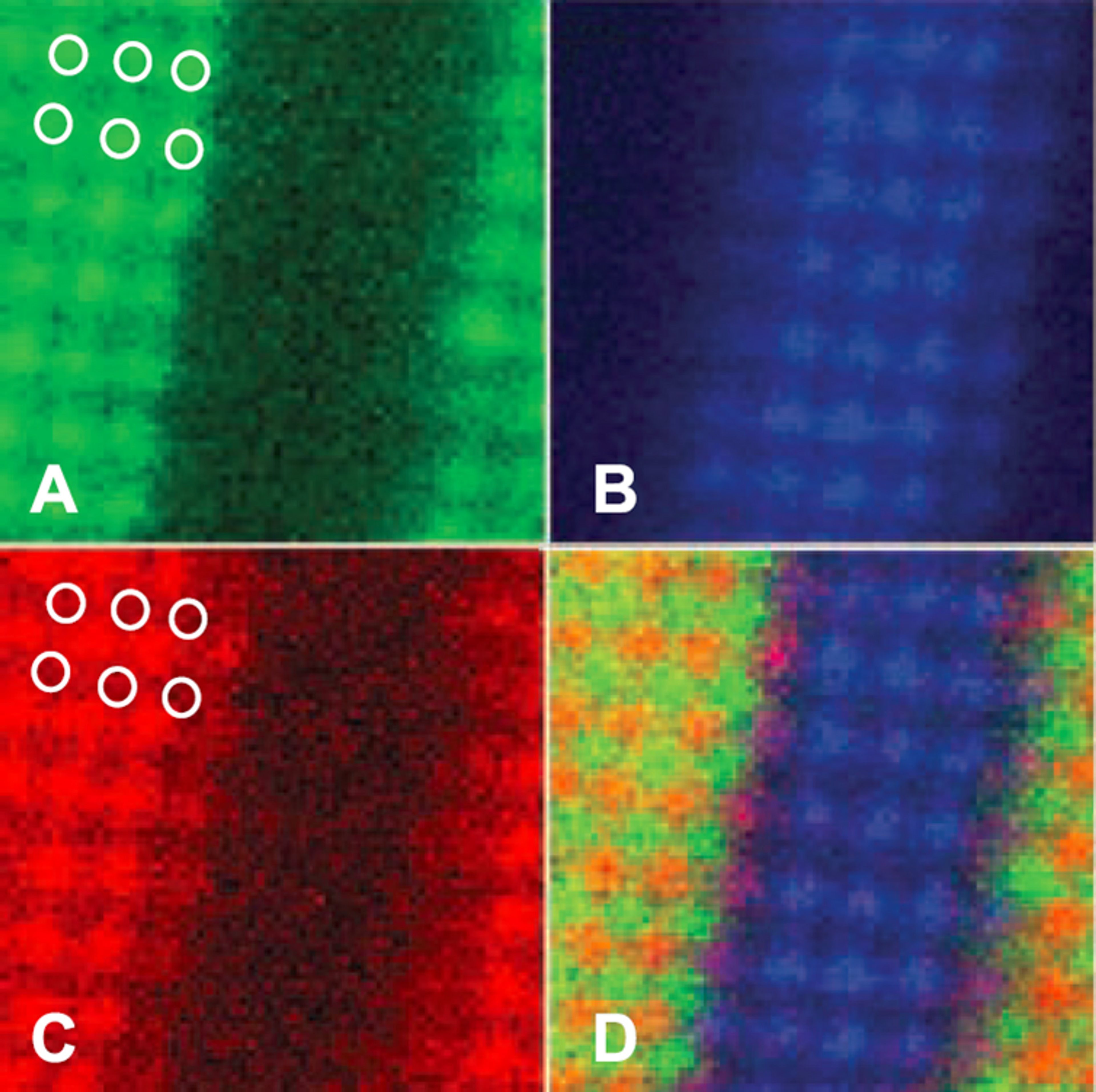
Figure 2. Atomic structure of different ferroelectric domains in the material PZT obtained by aberration-corrected TEM. The positions of the atoms (O, blue; Pb, yellow; Zr/Ti, red) in the two phases can be directly linked to the direction of electric polarization (Ps). Adapted from C.-L. Jia et al. Atomic-scale study of electric dipoles near charged and uncharged domain walls in ferroelectric films. Nature Μater. 7, 57–61 (2008); © Springer Nature Ltd


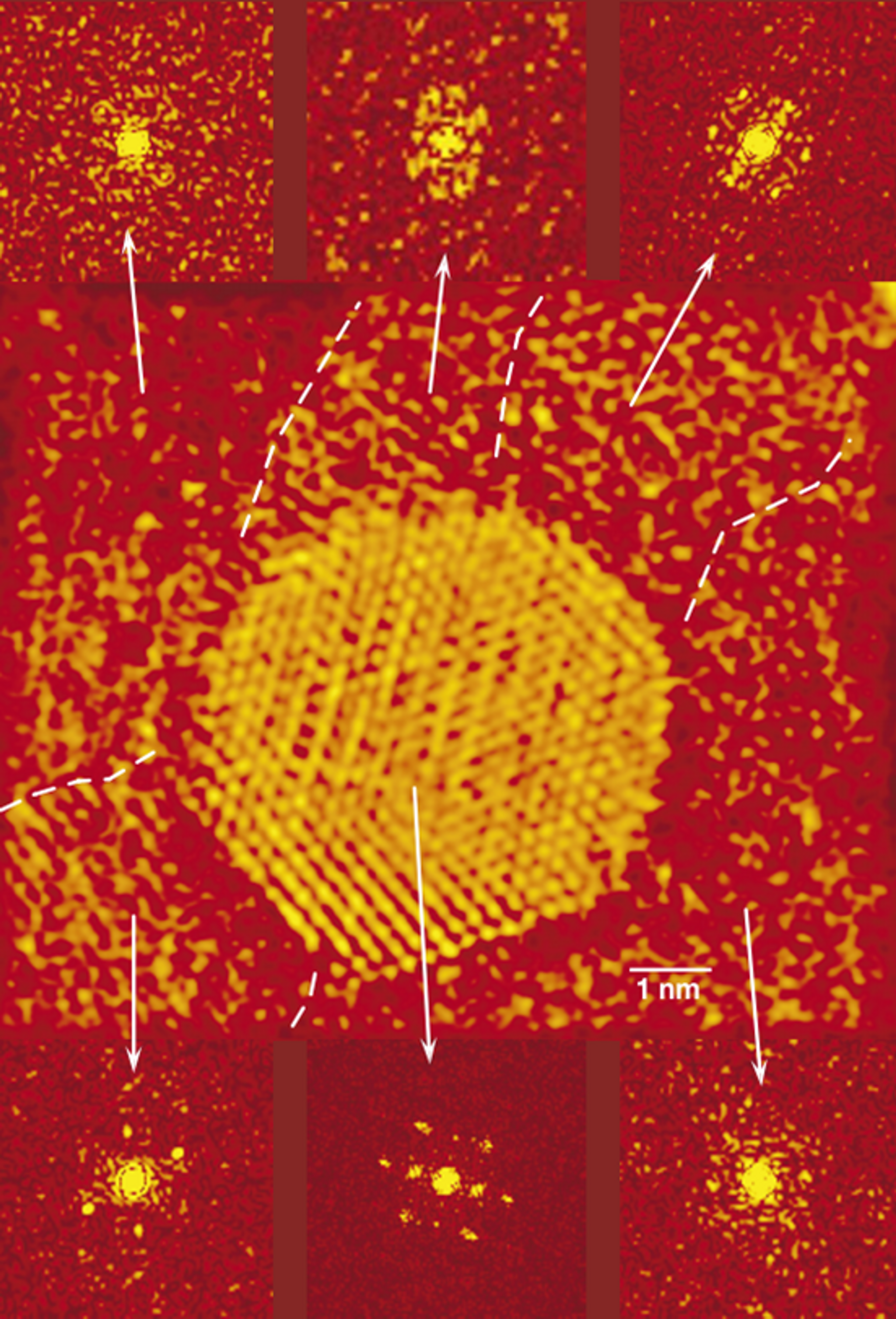
Figure 3. Atomic resolution image of an island of Au on an amorphous carbon substrate. The island is surrounded by monoatomic clusters of Au. Diffraction patterns from different regions surrounding the island show that these clusters are ordered in various structures adjacent to the built-up islands. Nature 418, 617-620 (2002); © Springer Nature Ltd.
While Rose, Haider and Urban were developing aberration-corrected CTEM, in 1995 Ondrej Krivanek, a long-time expert in electronic optics and EELS, started working in Cambridge, UK, with Mick Brown and Andrew Bleloch on the development of aberration correction in STEM. In 1997, together with Niklas Dellby, Krivanek started the company Nion to develop aberration-corrected STEM commercially. In 2002, Krivanek, Dellby and their colleague Phil Batson from IBM published sub-ångström resolution images (Figure 3) obtained with the Nion quadrupole-octupole STEM corrector.
The STEM has developed even further in the past two decades. As mentioned previously, the STEM can be used to perform EELS, and this combination has been used to obtain information on the chemical composition of materials (see Figure 4), and even on the type of bonding between atoms.
The pioneering work by Rose, Haider, Urban and Krivanek has now led to TEM and STEM instruments that are used routinely by research laboratories. Thanks to other advances, first and foremost the realization of highly sensitive electron detectors, both instruments can now be used on very delicate samples, including, for example, graphene and other two-dimensional materials. Some instruments are employed as mini-laboratories, where chemical reactions are carried out in-situ under direct atomic-resolution observation. There have also been attempts to go beyond imaging, and manipulate single atoms within a lattice. In industry, the instruments are regularly used to monitor the quality and reliable fabrication of devices. As Professor Bodil Holst of the University of Bergen, and chair of the Kavli Prize in Nanoscience Committee, said “Behind this year’s Kavli Prize lies more than 60 years of theoretical and experimental struggle. It is a beautiful example of scientific ingenuity, dedication and persistence. We honour four laureates who have enabled humanity to see where we could not see before”.


Figure 4. Atomic-resolution chemical map, obtained using EELS on an STEM, of a (La,Sr)MnO3/SrTiO3 multilayer showing the La (green), Ti (blue) and Mn (Red) atoms; the white circles indicate the position of the La columns; field of view 3.1 nm. From D. A. Muller et al. Atomic-scale chemical imaging of composition and bonding by aberration-corrected microscopy. Science 319, 1073–1076 (2008).
The first electron microscopes enabled scientists to finally view the nanoworld. But because of limitations in the microscope's lenses, achieving sharp images of individual atoms was not possible. For 60 years scientists struggled with the scopes' limited abilities.
The 2020 Kavli Prize In Nanoscience is awarded to Harald Rose, Ondrej Krivanek, Maximilian Haider, and Knut Urban for their work in sub-ångström resolution imaging and chemical analysis using electron beams.