


2016 kavli prize in Nanoscience
2016 Kavli
Prize in
Nanoscience
The Norwegian Academy of Science and Letters has decided to award the 2016 Prize Kavli in Nanoscience to Gerd Binnig, Christoph Gerber and Calvin Quate.


“For the invention and realization of atomic force microscopy, a breakthrough in measurement technology and nanosculpting that continues to have a transformative impact on nanoscience and technology.”
Committee Members
- Arne Brataas (Chair), The Norwegian University of Science and Technology, Norway
- Mildred Dresselhaus, Massachusetts Institute of Technology, USA
- Laura H. Greene, University of Illinois at Urbana-Champaign, USA
- Jochen Mannhart, Max Planck Institute for Solid State Research, Germany
- Ke Lu, Institute of Metal Research, Chinese Academy of Sciences, China
Citation from the committee
Sculpting and analysing nanoscale structures are at the core of nanoscience. An ultimate dream had been to position atoms on any surface, one by one, to enable the design and creation of revolutionary new structures. Imaging atomic structures in a wide range of material systems was another visionary concept. The invention of atomic force microscopy has turned these dreams into reality. Atomic force microscopy is now widely used in the fields of physics, chemistry, biology, and materials science.
In atomic force microscopy, a nanoscale tip scans across a sample surface at atomically close range. At the same time, the tiny forces between the sample and the tip are detected. These forces reveal many properties of the sample, such as the arrangement of its individual atoms, now with subatomic resolution. Electric and magnetic interactions, friction, and chemical bonding can induce these forces. The technique is applicable over a wide temperature range and in magnetic fields. Unlike scanning tunnelling microscopy, atomic force microscopy can also be applied to insulating materials.
Nanosculpting refers to adding, arranging, and removing atoms to produce desired phenomena and functions. The tip provides a versatile tool for accomplishing such control. Being able to manipulate conductors and insulators at the nanoscale has applications comparable to those of nanoscale 3D printing. Nanostructures created by force microscopy-based techniques include devices in nanoelectronics, nanophotonics, and nanomagnetism.
The advantages of atomic force microscopy include experimenting in liquids such as water, which opens the possibility of exploring biological systems. A single molecule, such as a DNA or a protein molecule, can be suspended between the tip and surface. Lifting the tip stretches and unfolds the molecule. The measured restoring force reveals the molecule’s elastic properties and functionality. Biochemical sensors are utilizing the in-situ detection of chemical reactions by temperature-sensitive cantilevers, opening new doors for medical applications. In life sciences, explorations of molecular processes with high resolution advance drug design.
The invention of atomic force microscopy has spawned a wide variety of measurement and manipulation techniques invaluable for many purposes. These range from magnetic force and chemical force microscopy to magnetic resonance spectroscopy, and scanning capacitance microscopy. Another example is friction force microscopy that deepens our understanding of lubrication at the atomic level.
Atomic force microscopy is a powerful and versatile scientific technique that continues to advance nanoscience for the benefit of society.
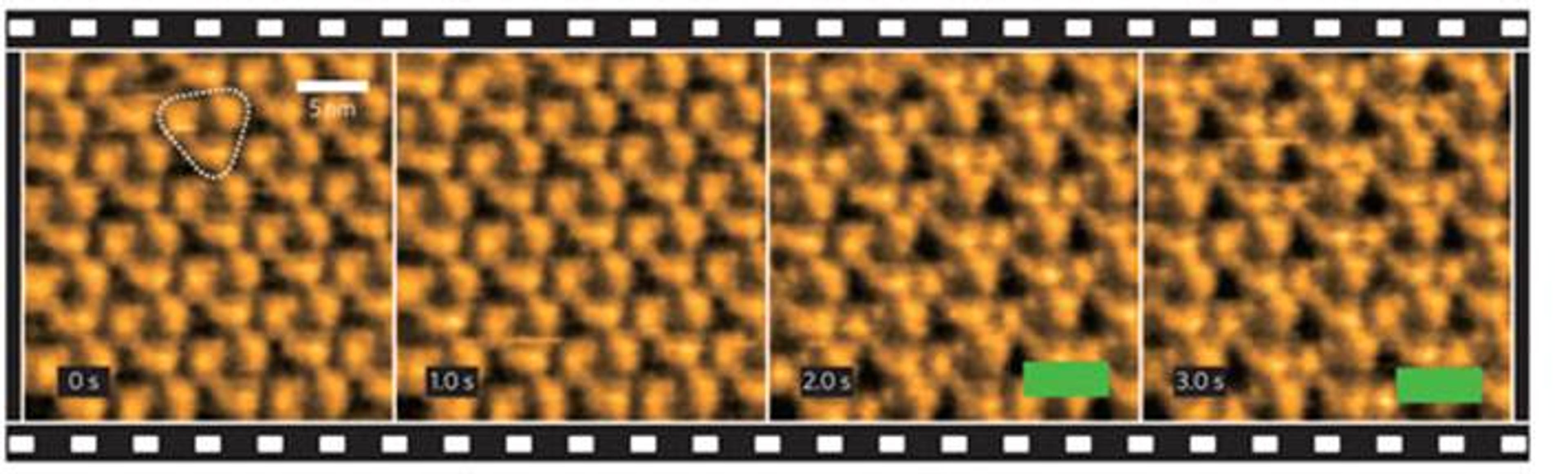
Successive high-speed AFM images of bacteriorhodopsin proteins adsorbed onto a mica surface. (Photo credit: Reprinted by permission from Macmillan Publishers Ltd: Nature Nanotechnology 5, 208-212 (2010)).
A scanning microscope for all surfaces
The ability to image matter with atomic resolution and to modify the properties of materials by moving atoms one by one are among the ultimate goals of nanoscience.
By Fabio Pulizzi, science writer/editor
In making their award, the Kavli Prize in Nanoscience committee has selected three scientists who first realized an instrument that could provide images of surfaces of any type of material with a resolution of fractions of nanometres — one that is used today in a variety of scientific fields for imaging and manipulation.
Towards the end of the 1970s, efforts to push the limits of imaging resolution had led to very promising results. Although the resolution of optical microscopy is limited to fractions of micrometres, developments in near-field microscopy had pushed this limit to a few tens of nanometres. Advances in electron microscopy had also enabled a resolution of a few nanometres to be reached, although this was based on high-energy electron beams that could damage the materials being studied.

The first atomic force microscope, 1985. Made by Calvin Quate and Gerd Binnig of Stanford University, and Christoph Gerber of IBM Research. Photo: Science & Society Picture Library/Getty Images.
The turning point came in 1981, when scientists at IBM Zürich, led by Gerd Binnig and Heinrich Rohrer, realized the scanning tunnelling microscope (STM). This instrument consists of a conductive tip that is placed at such a small distance from a conductive sample that a current flows between the tip and the sample. Because the current depends very sensitively on this distance, by scanning the tip over the sample surface it is possible to obtain an image of the surface with a resolution of only a few nanometres.
Despite its immense potential, the STM only works on conductive samples. Gerd Binnig came up with an idea to modify it and create an instrument that would provide images of all types of sample, conductive or insulating, and in 1985 filed a patent for an instrument that he called the atomic force microscope (AFM). The ingenious modification was to place a conductive cantilever, terminated by a tip, just under the tip of an STM. The current between the cantilever and the STM tip would therefore vary with the vertical movement of the cantilever. By scanning the cantilever over the sample’s surface, the vertical movement of the cantilever, hence the profile of the sample, could be recorded by monitoring the changes in current.
The idea seemed simple enough, so Gerd Binnig involved Calvin Quate from Stanford University — where Binnig himself was temporarily working — and his IBM colleague Christoph Gerber, with whom he had already collaborated for the development of the STM, and together they realized the AFM along the lines proposed by Binnig in his patent (Fig. 1). The results of their experiments are described in a paper published in Physical Review Letters in March 1986. As the three scientists explain, the cantilever moves because of the finite though small interaction between electrons associated with atoms on the surface and those in the tip attached to the cantilever. For the movement to be large enough to be detected, the cantilever needs to have a small mass and a small spring constant. The AFM was tested using different combinations of experimental conditions, and they managed to obtain a surface profile with a lateral resolution of 30 Å and a vertical resolution of less than 1 Å.

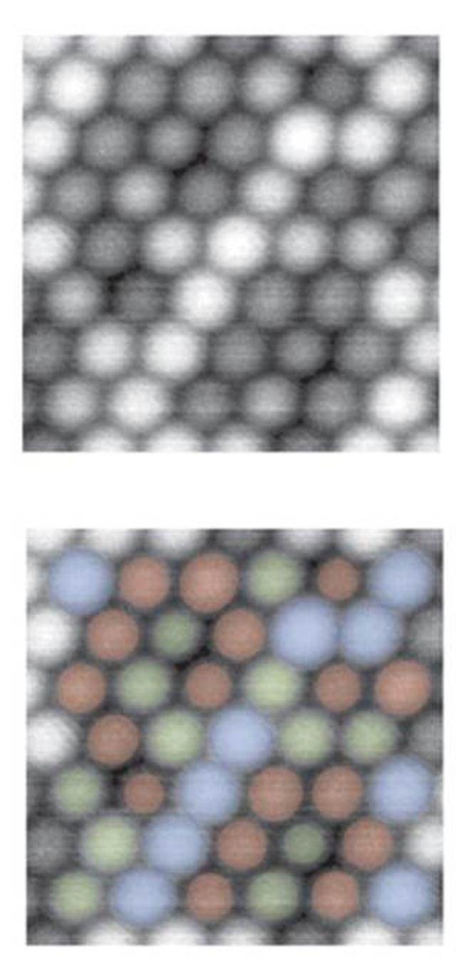
AFM images of Sn, Pb and Si atoms on a Si(111) surface. The atoms can be distinguished in the top image by their size and brightness. The bottom panel reproduces the top one, but with added colour in the centre part of the image to distinguish between Sn (blue), Pb (green) and Si (red) atoms. Reprinted by permission from Macmillan Publishers Ltd: Nature 446, 64-67 (2007).
The instrument reported in the Physical Review Letters paper is now known as a contact mode AFM. Major developments in instrumentation that followed were the demonstration of non-contact mode AFM in 1987 and tapping mode AFM in 1993, which is probably the most common way in which AFMs are used today. In this mode the tip oscillates over the sample, occasionally tapping it for a short enough time to avoid damage to the surface while still measuring topology and interaction between the tip and the surface; this measuring mode would become essential for studies of biological samples. Also in the early 1990s, a new technique was introduced to monitor the deflection of the cantilever in an AFM through the reflection of a laser, rather than through an STM signal.
Advances in sensitivity and resolution as well as developments in modelling and analysis led to milestones in the experimental studies of chemical bonds using AFM. In 2007, scientists in Japan, Spain and the Czech Republic were able to identify individual atoms of different elements, namely Sn, Pb and Si, deposited on a Si(111) surface (Fig. 2). In 2009, scientists at IBM used an AFM with a CO2 molecule adsorbed on the tip, and using the interaction of this molecule with carbon atoms, they were able to resolve with high detail the chemical structure of small molecules like pentacene. Using the same technique, a few years later they succeeded in distinguishing different types of chemical bond between carbon atoms in a hydrocarbon molecule.
The AFM has also had wide use in biology by allowing high-resolution images of a variety of membranes, viruses and bacteria. Furthermore, the instrument can be employed to measure the force between the tip and a surface, and in some cases even the force between a molecule stuck to the tip and other molecules in a biological tissue. This has allowed investigation of the mechanical properties of cells, which, according to some research studies, could have applications in medicine, for example by enabling cancer cells to be distinguished from healthy ones. In genetics, both high-resolution imaging and force microscopy have been used to study the DNA–RNA polymerase interaction, as well as to identify small defects in chromosomes. Finally, the realization of short but soft cantilevers, as well as other improvements in instrumentation, have led to the development of high-speed AFM, which enables a biological process to be followed in real time, for example the movement of individual proteins in biological membranes (Fig. 3).

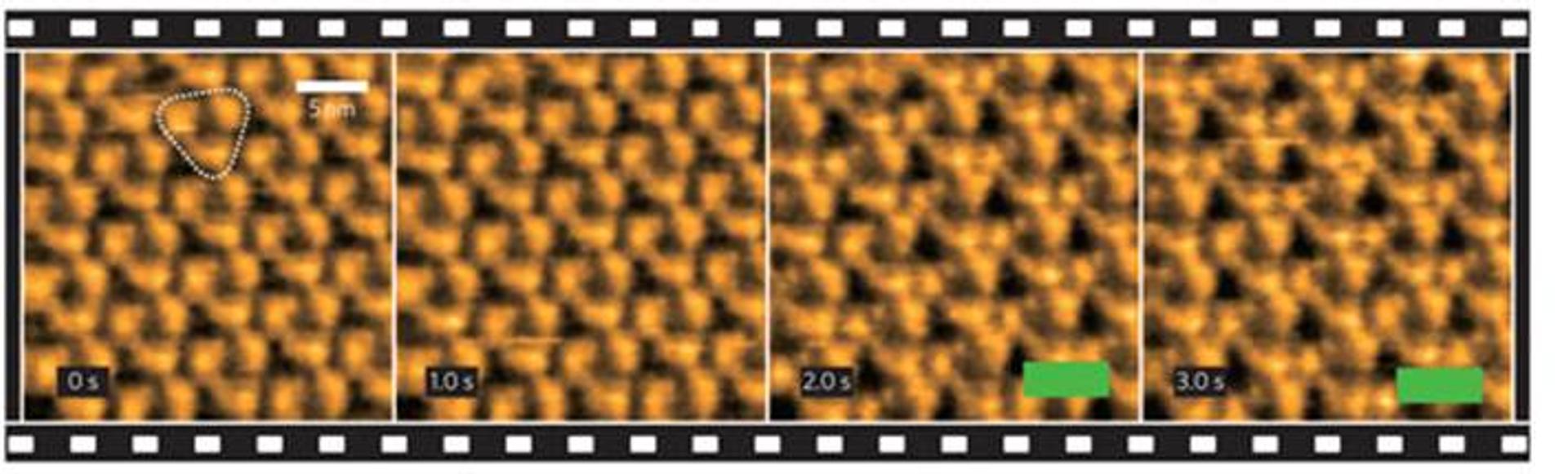
Successive high-speed AFM images of bacteriorhodopsin proteins adsorbed onto a mica surface. Reprinted by permission from Macmillan Publishers Ltd: Nature Nanotechnology 5, 208-212 (2010).
The AFM is not only a measuring and imaging instrument. In the last few years, it has been shown that the tip of the instrument can be used to modify the surface of materials with atomic precision. Initial experiments have shown that it is possible to swap an atom of Sn deposited on a Si surface with an atom of Si adsorbed on an AFM tip (Fig. 4). The tip can also be used to move atoms adsorbed on surfaces by literally pushing them from one adsorption site to the next.
More generally, AFM is at the basis of a number of techniques known collectively as scanning probe lithography. For example, a conductive tip can be used to write patterns on different materials by locally oxidizing or reducing a surface, a method that has been used to create conductive channels in, for example, graphene and oxide interfaces. In dip-pen nanolithography, the AFM tip is used to write patterns by depositing liquids of different types. Alternatively, the tip of the AFM can be used to locally heat up polymer-based surfaces and create patterns by removal of atoms.
In their 1986 paper, Binnig, Quate and Gerber had simply reported profile lines of an Al2O3 surface, but the legacy that their work has left, thanks also to further developments by other scientists, has been immense. As Professor Arne Brataas, of the Norwegian University of Science and Technology, and chairman of the Kavli Nanoscience Prize Committee said “Atomic force microscopy is a powerful and versatile scientific technique that continues to advance nanoscience for the benefit of society.”